HVeVR2
HVeV Run 2
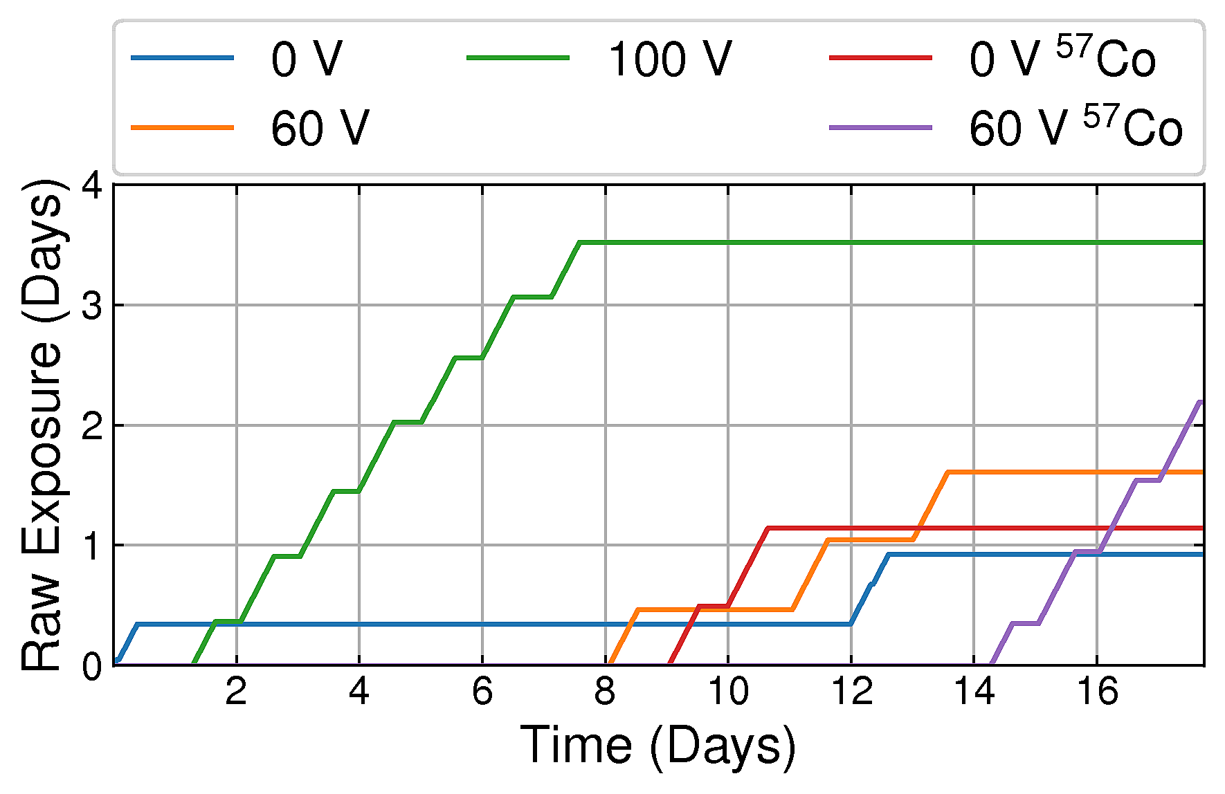
Abstract This Public Documentation accompanies the results on electron-recoiling dark matter (ERDM) from a 3 week long run of a 1g HVeV detector in the Northwestern ADR. During this run, one week of data (roughly 12 hours per day for 7 days) was acquired at 100V bias with a charge resolution of 0.03 electron-hole pairs, and 3 days at 60V with a resolution of 0.05 electron-hole pairs. Co-57 and laser calibrations were acquired, and a 0V control sample was also acquired over multiple days. The resulting limits for DM-electron scattering and DM absorption are given below, along with plots approved for public release.
These results are availiable from arXiv:2005.14067
All results assume a relic DM density of ρDM = 0.3 GeV/cm3. All limits are at 90% confidence level. σe is the DM-electron scattering cross section. FDM is the DM form factor where FDM = 1 (FDM ∝ 1/q2) corresponds to a DM model with a heavy (ultra light) dark photon mediator. q is the momentum transfer. mDM is the DM mass. More detailed information on the assumed DM models and astrophysical parameters can be found in the US Cosmic Visions Community Report.
Result
Topic
Last Updated
Comments/Download


Experimental Setup
August 16th, 2019

Experimental Setup
January 30th, 2020

Experimental Setup
January 30th, 2020
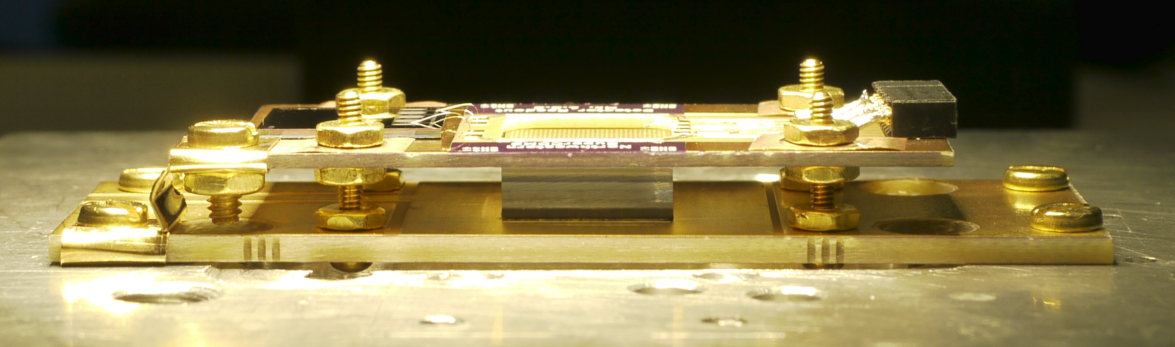
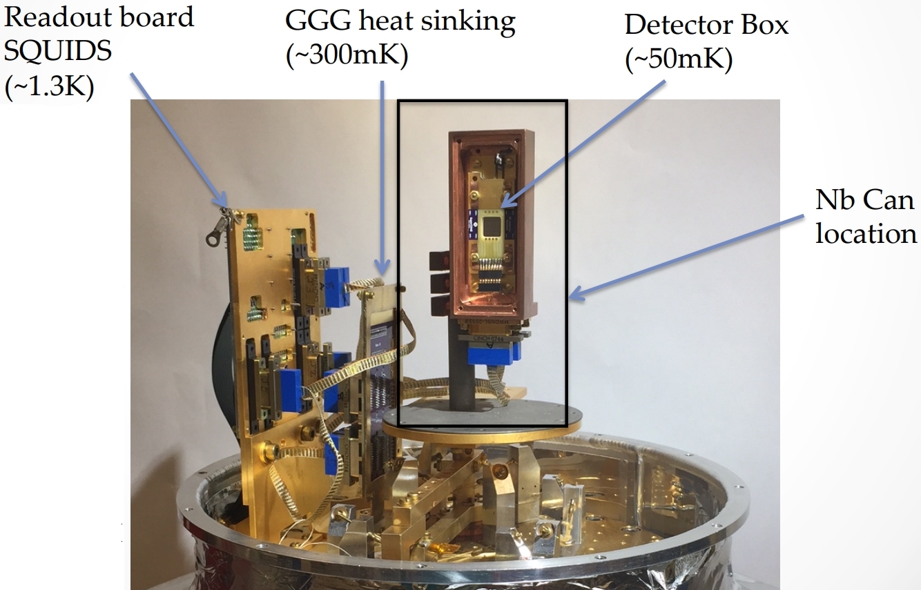
Photograph of the HVeV R2 detector installed in the ADR
Picture of the HVeV detector installed in the ADR at Northwestern University. (ArXiv:1903.06517). The ADR has two salt pills, GGG operating around 300 mK and FAA operating around 50 mK. The detector is thermally linked to the FAA salt, with temperature stabilized to 50 mK or 52 mK during the operation. A superconducting magnetic field shield, the Nb can, is mounted on the FAA stage around the detector box. The cold electronic readout device, SQUIDs, are mounted on a thermal stage operated at 1.3 K.

Experimental Setup
January 30th, 2020

Experimental Setup
February 21st, 2020

Data Acquisition
February 21st, 2020

Detector Response
February 21st, 2020
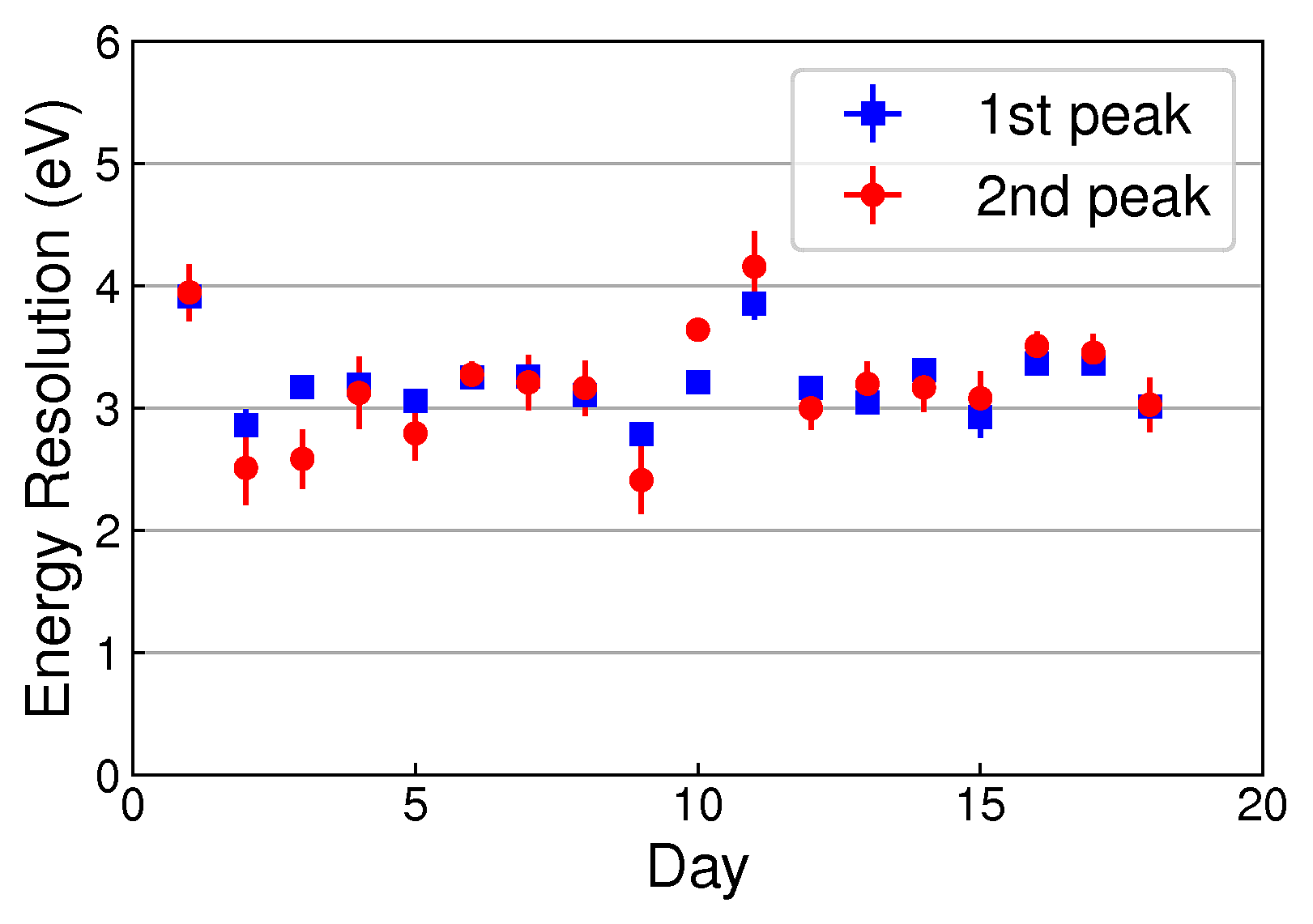
Phonon resolution on each day of acquisition
Phonon resolution as measured using laser calibration data for each day of Run 2. Variations are due to noise changes and change in TES bias point day to day. With a few exceptions, we consistently achieve a resolution of ~3.2 eV in the first electron-hole peak. The first point is inconsistent with the others because of an excessively noisy power supply that was replaced starting day 2.

Detector Response
February 21st, 2020
Charge resolution on each day of acquisition
Charge resolution as measured using laser calibration data for each day of Run 2. Variations are due to changes in noise, but largely are determined by the voltage bias used for each calibration as expected due to NTL gain. Resolution for points at the same bias are consistent throughout the run. The first point is inconsistent with the others because of an excessively noisy power supply that was replaced starting day 2.

Detector Response
February 21st, 2020
Relative gain.
Scatter plot comparing the inner and the outer channel for one day of background data: both channel have the same gain thanks to the same-area sensor design of the TES mask. The two anti-diagonal dashed lines indicate the first (lower left) and the second (upper right) electron-hole pair peaks.

Detector Response
February 21st, 2020

Detector Response
February 21st, 2020
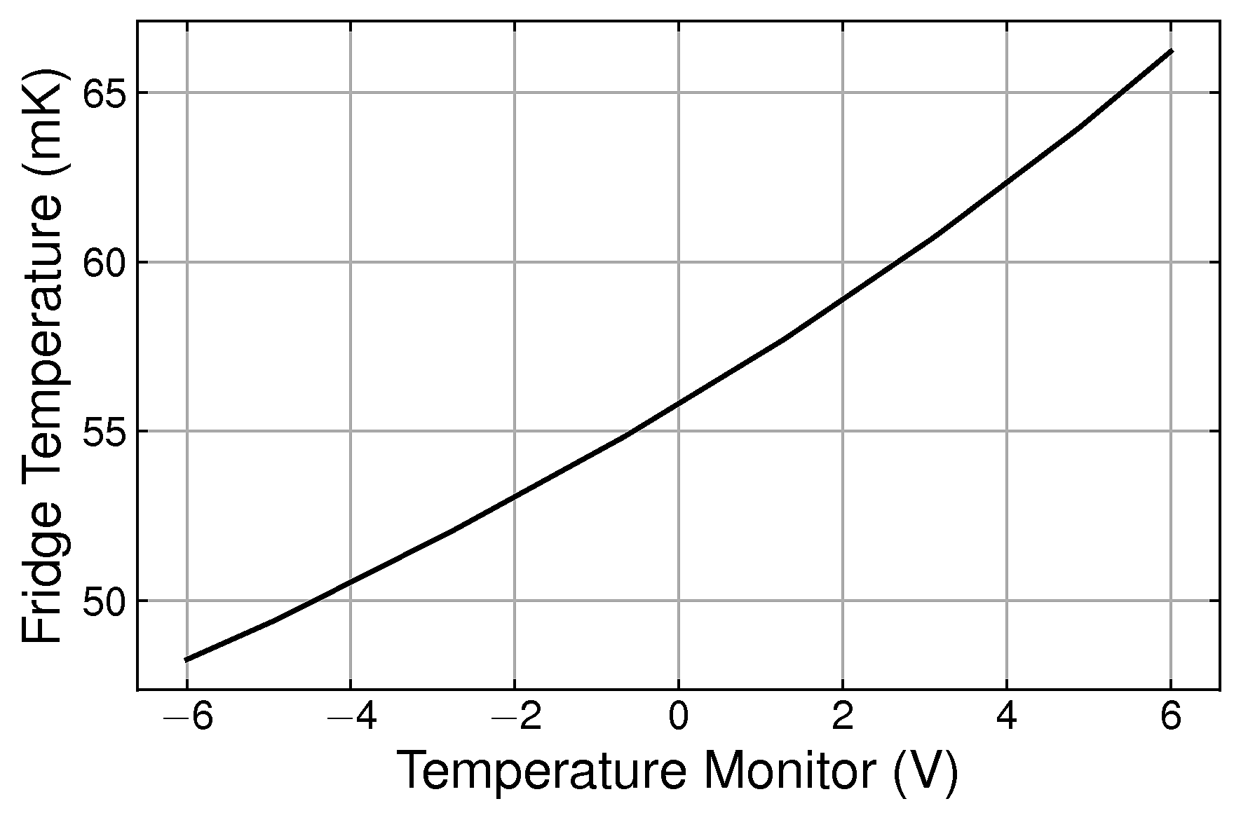
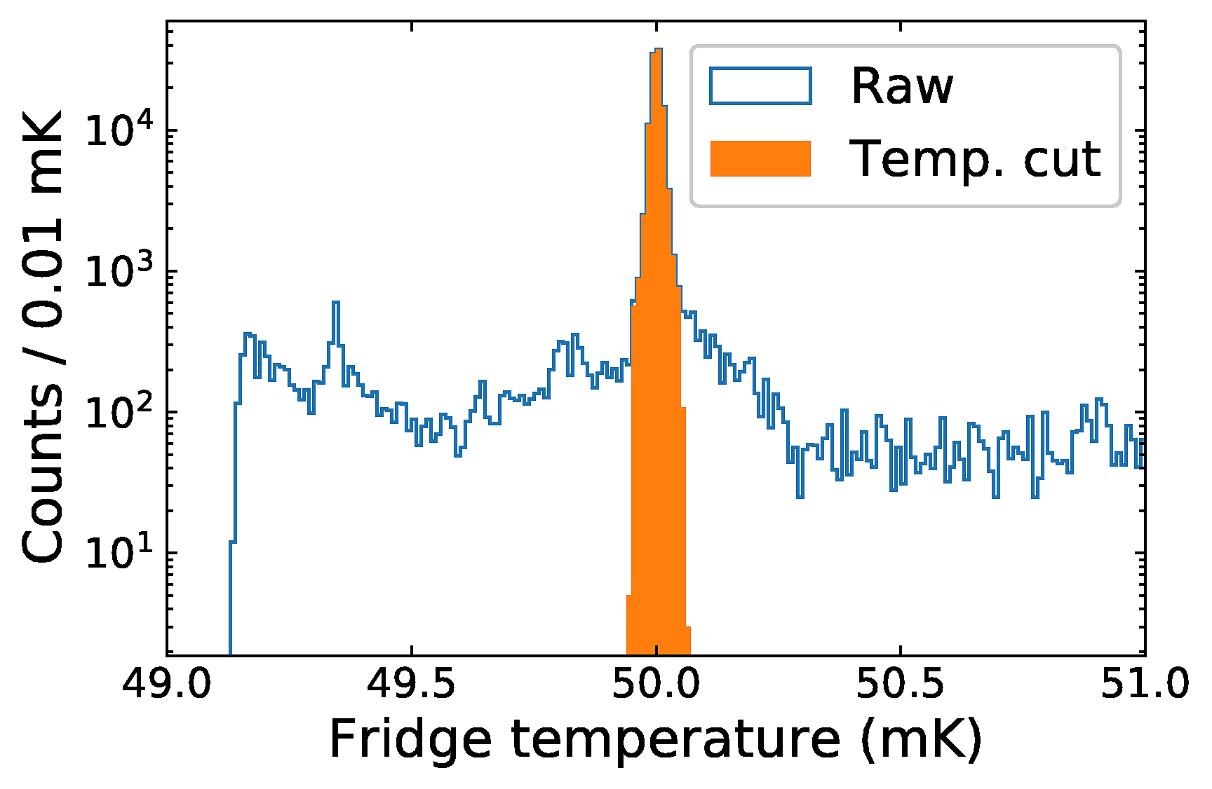
Base temperature during data taking as a function of time.
Temperature was stabilized at 50 mK during the run for the first 9 days, after which it was raised to 52 mK in order to increase hold time. Periodic deviations in temperature can be seen, as well as rises in temperature at the end of each day as the fridge runs out of cooling power. Light/yellow-ish colors refer to a high count density and dark/purple colors refer to a low count density.

Detector Response
February 21st, 2020
Laser amplitude as a function of the temperature for twelve series acquired at different temperatures.
We acquired twelve laser series at different temperatures in order to correct for gain variations due to temperature instabilities and drifts. This plot shows the peak position fitted from the laser data as a function of the temperature.

Detector Response
February 21st, 2020
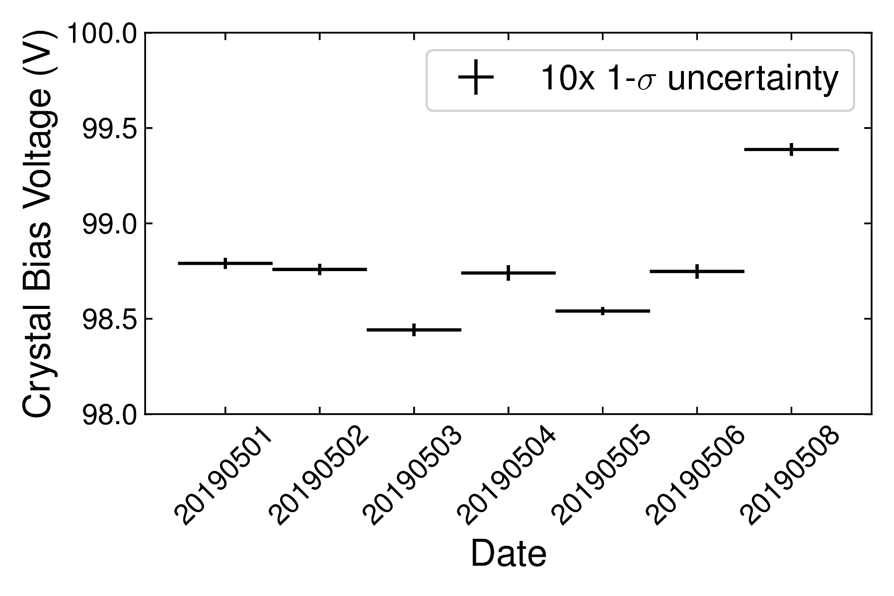
Spread of the HV applied on the detector for different series.
The HV was set each day by hand with a knob and it was recorded each second by the DAQ. We found differences between the average values set each day and we corrected for them in the HV correction. The uncertainties are present in this plot but they are so small that are not visible.

Detector Response
February 21st, 2020
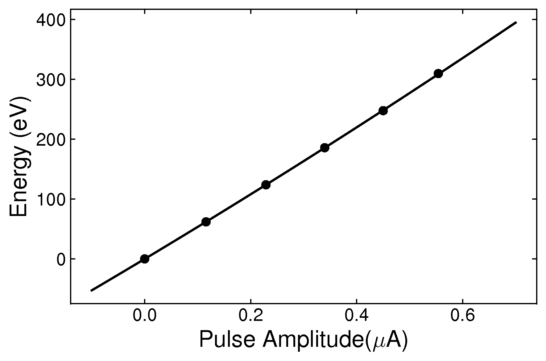
Linearity correction and calibration.
The linearity correction and calibration of the HVeV R2 detector was done with the laser data acquired daily. This plot - showing the energy as a function of the optimum filter amplitude - is an example of the curve used for the calibration and linearity correction in one day.

Data
February 21st, 2020
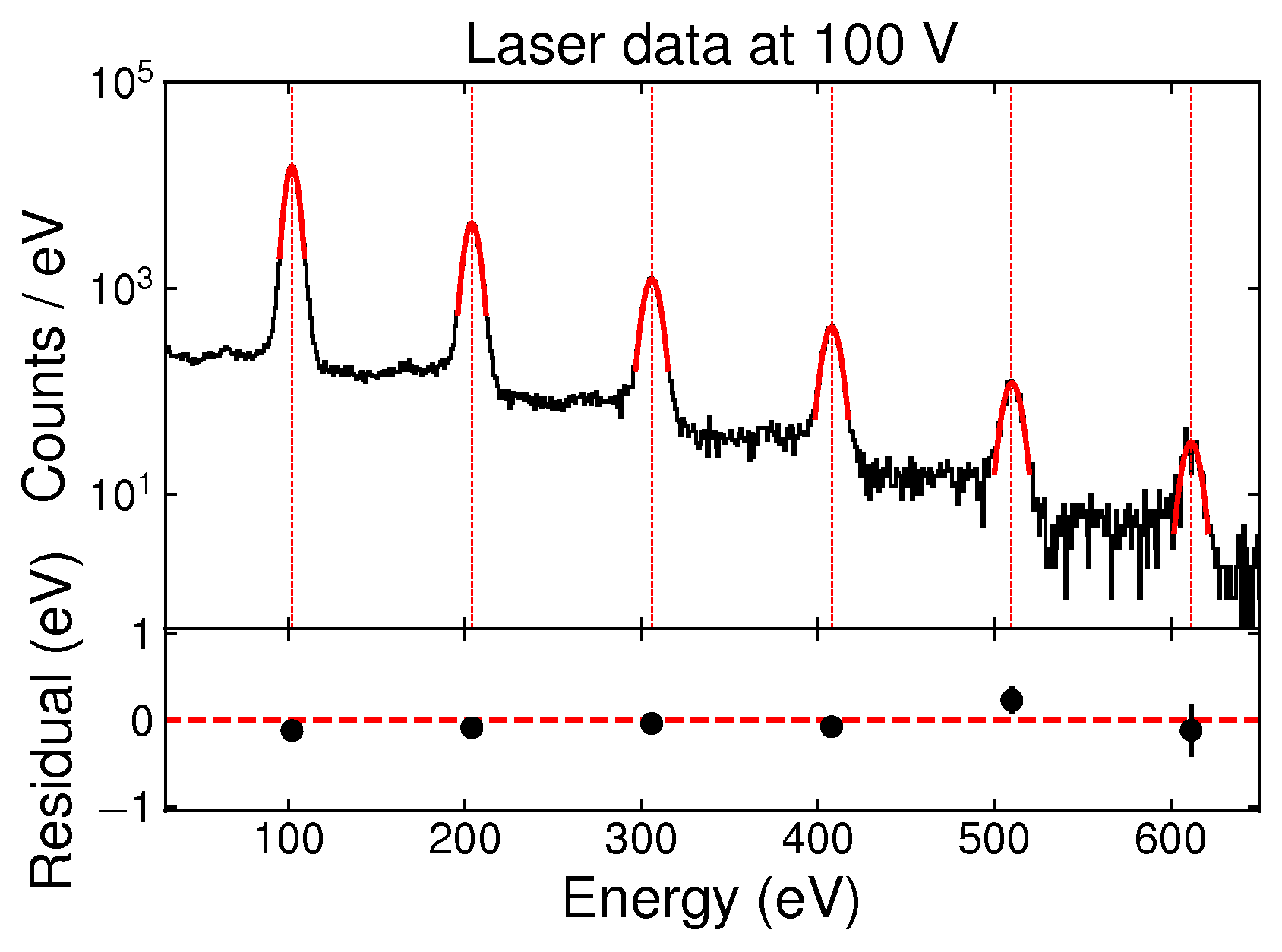
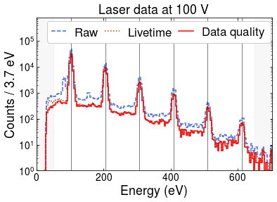
Combined laser spectra after the corrections and calibration for the 100 V data
Top panel: combined spectra of laser data (black histogram) at 100 V after the corrections (temperature, high voltage, QET absorption, linearity) and the calibration. The red curves represent Gaussian fits to each individual peaks. The expected peak positions are multiples of the photon energy (1.95 eV) plus the NTL gain energy for 1 electron-hole pair (100 eV). Bottom panel: residuals between the laser peak position after the calibration and the expected value.

Data
February 21st, 2020
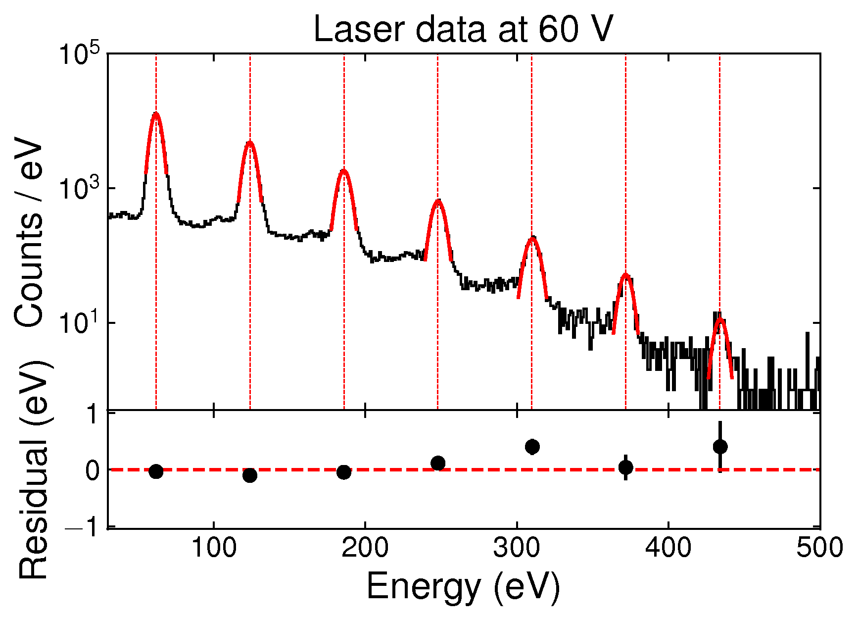
Combined laser spectra after the corrections and calibration for the 60 V data
Top panel: combined spectra of laser data (black histogram) at 60 V after the corrections (temperature, high voltage, QET absorption, linearity) and the calibration. The red curves represent Gaussian fits to each individual peaks. The expected peak positions are multiples of the photon energy (1.95 eV) plus the NTL gain energy for 1 electron-hole pair (60 eV). Bottom panel: residuals between the laser peak position after the calibration and the expected value.

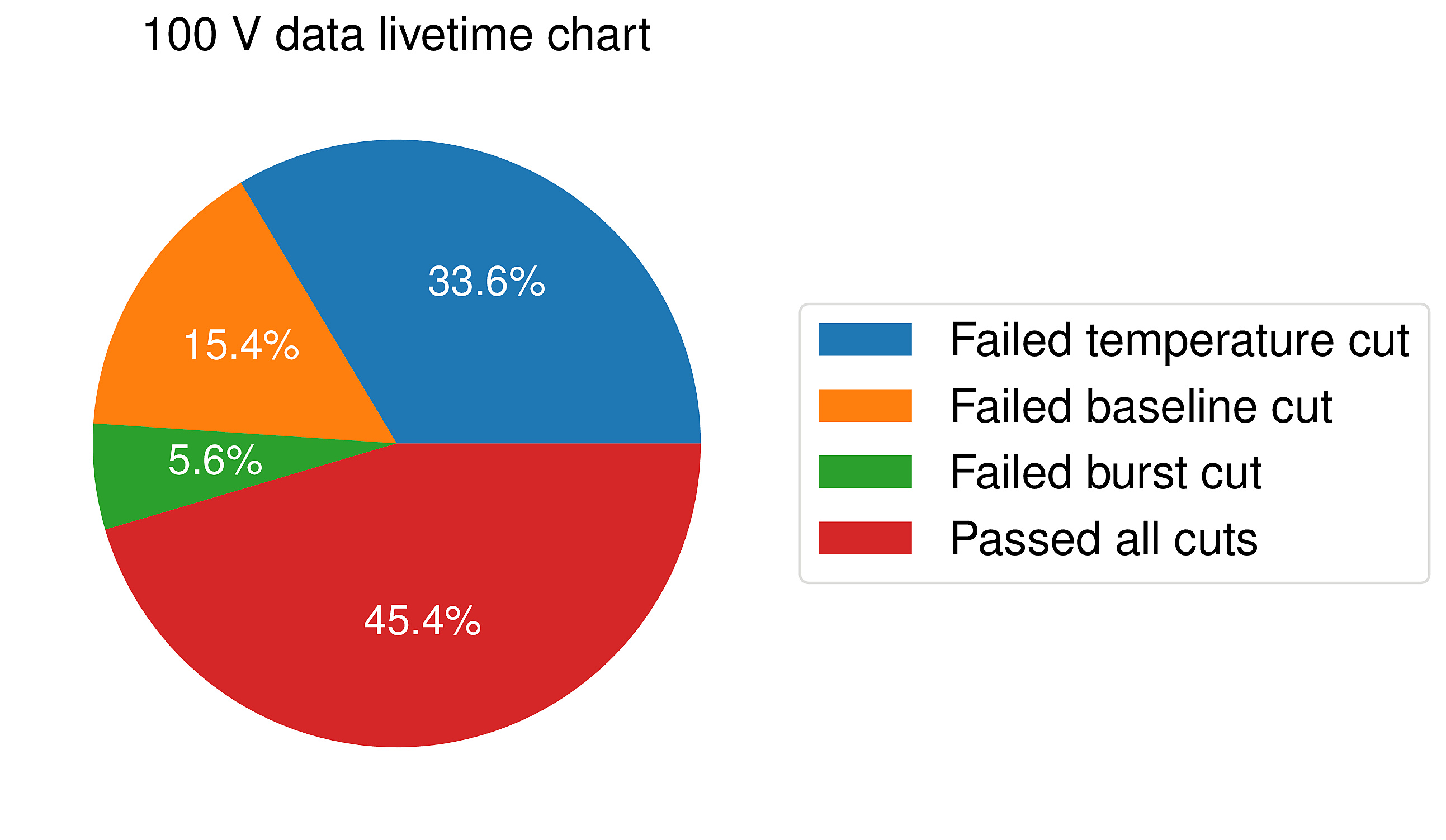
Livetime cuts
February 21st, 2020

Livetime cuts
February 21st, 2020

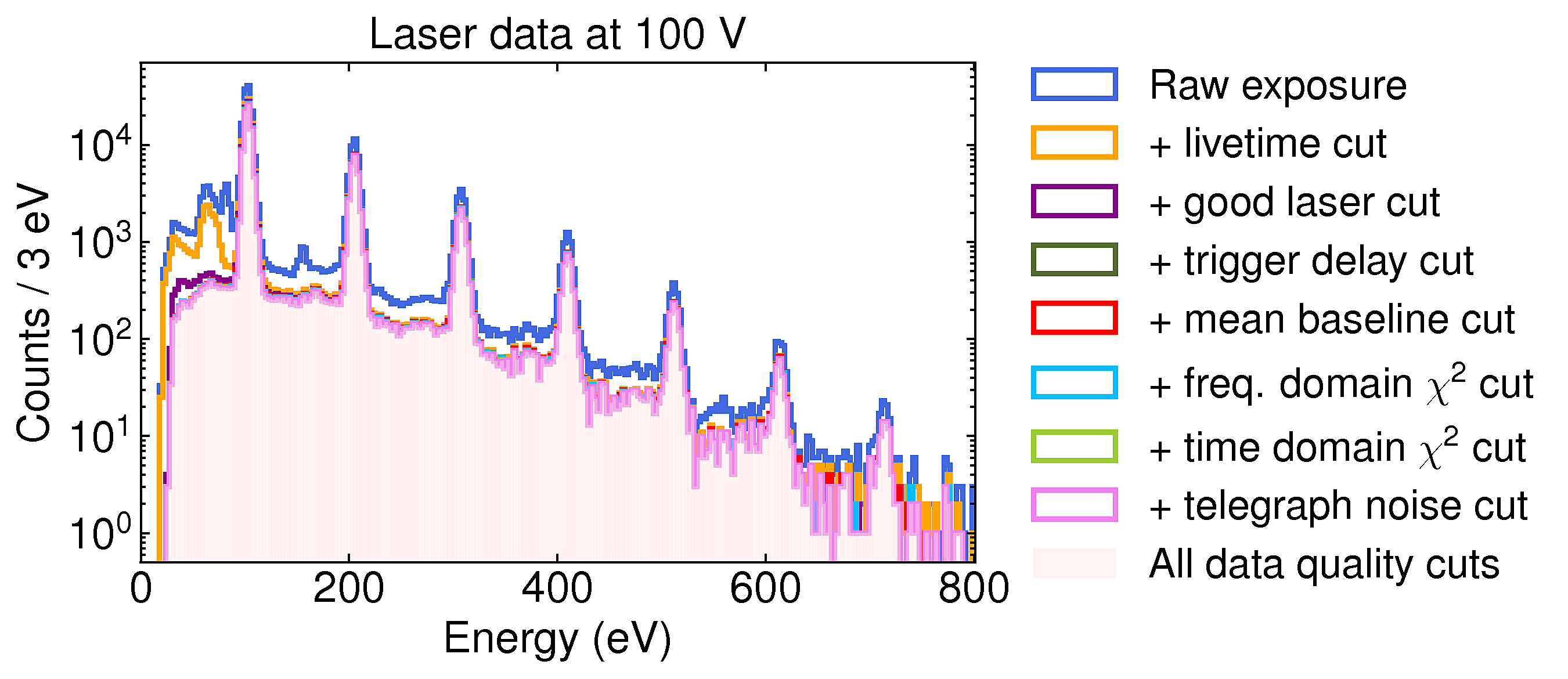
Data quality cuts
February 21st, 2020
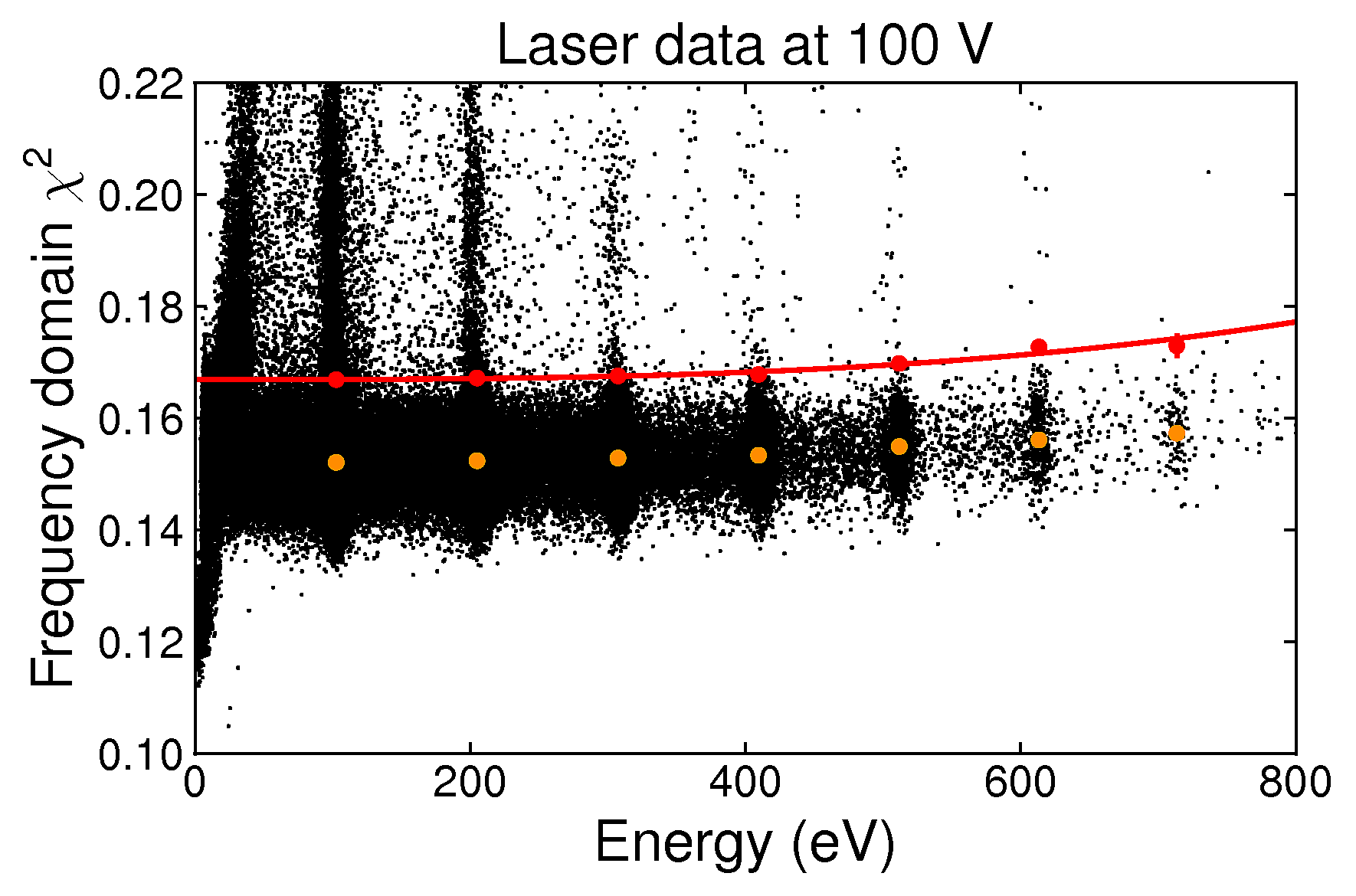
Frequency-domain Χ2 cut for the 100 V data
The frequency-domain Χ2 cut belongs to the data quality cuts and was studied with the laser data. This plot shows the frequency-domain Χ2 as a function of the energy. The orange dots represent the peak of the Χ2 distribution for each electron-hole pair peak. The red dots represent 3σ position of the corresponding peak. The red line corresponds to the position of the cut.

Data quality cuts
February 21st, 2020
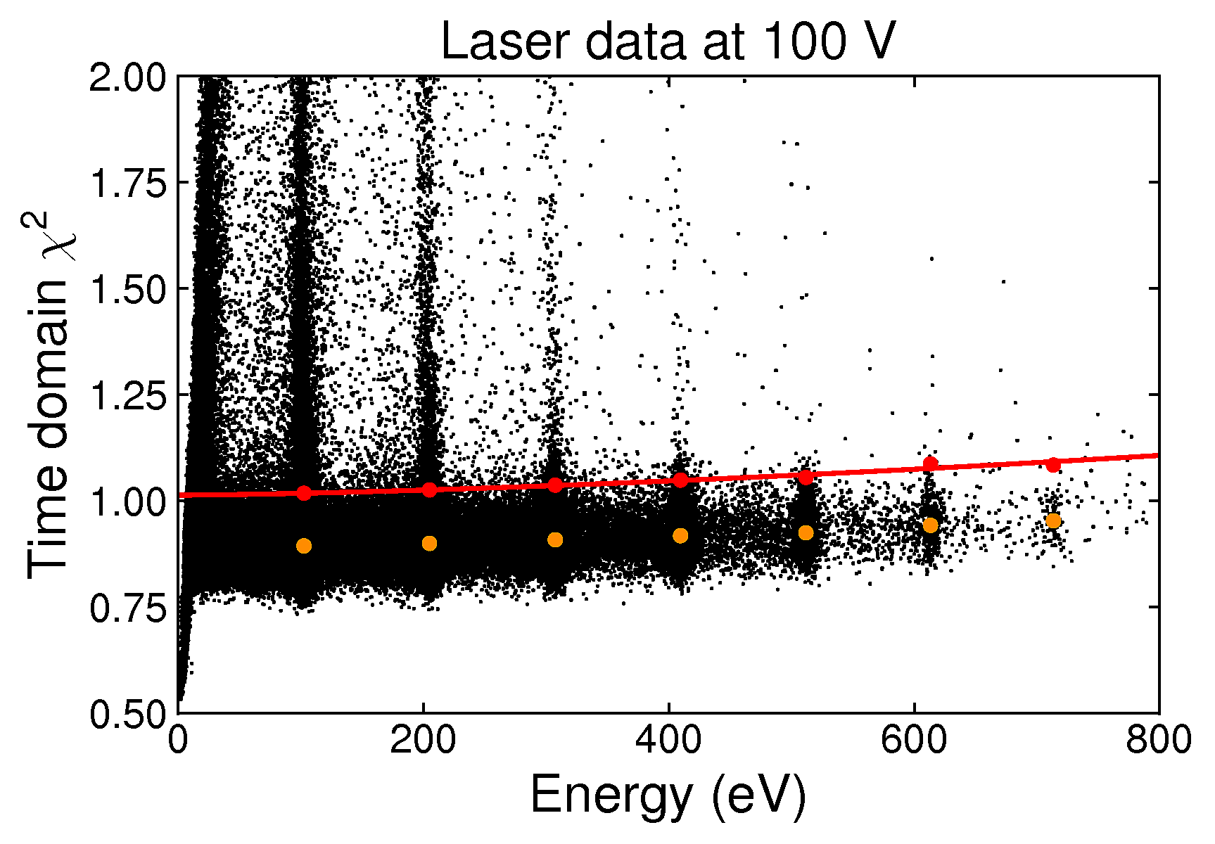
Time-domain Χ2 cut for the 100 V data
The time-domain Χ2 cut belongs to the data quality cuts and was studied with the laser data. This plot shows the time-domain Χ2as a function of the energy. The orange dots represent the peak of the Χ2 distribution for each electron-hole pair peak. The red dots represent 3σ position of the corresponding peak. The red line corresponds to the position of the cut.

Data quality cuts
February 21st, 2020

Trigger
February 21st, 2020
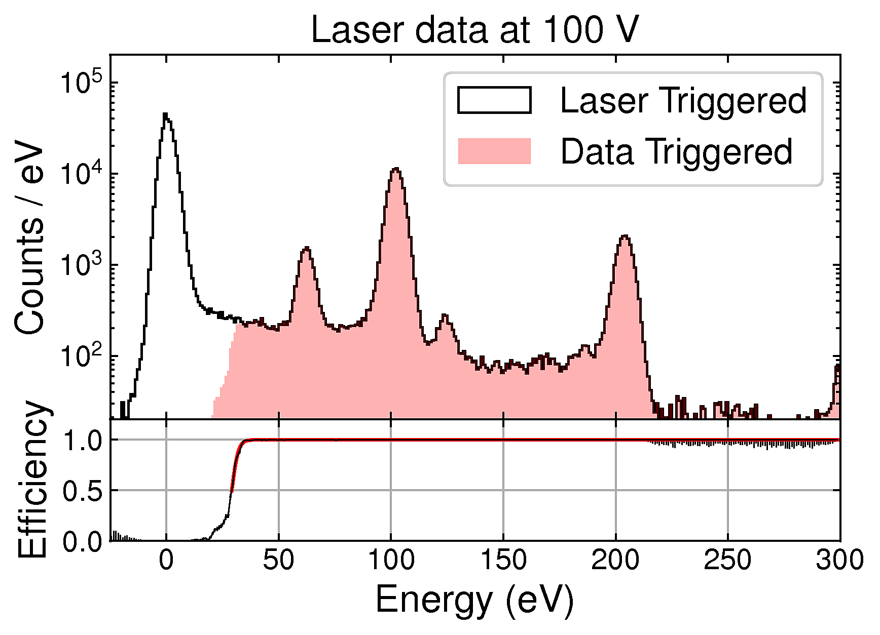
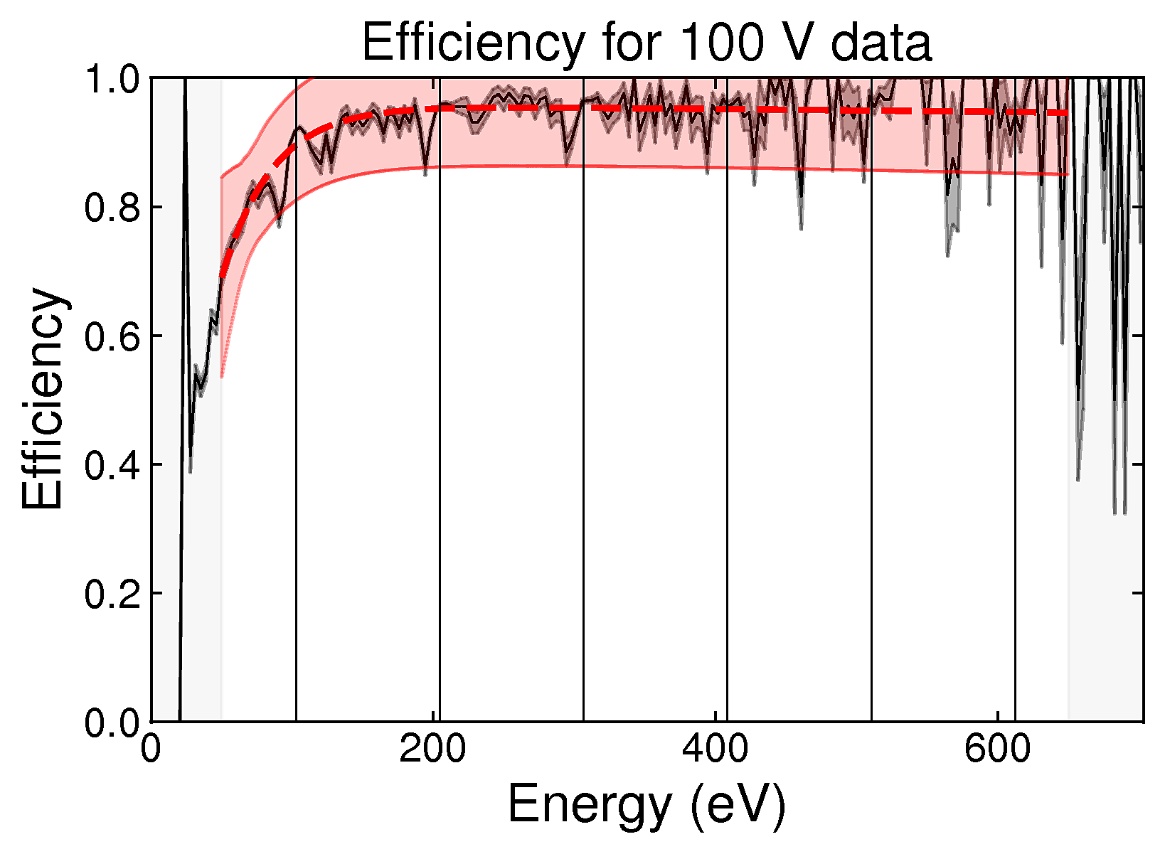
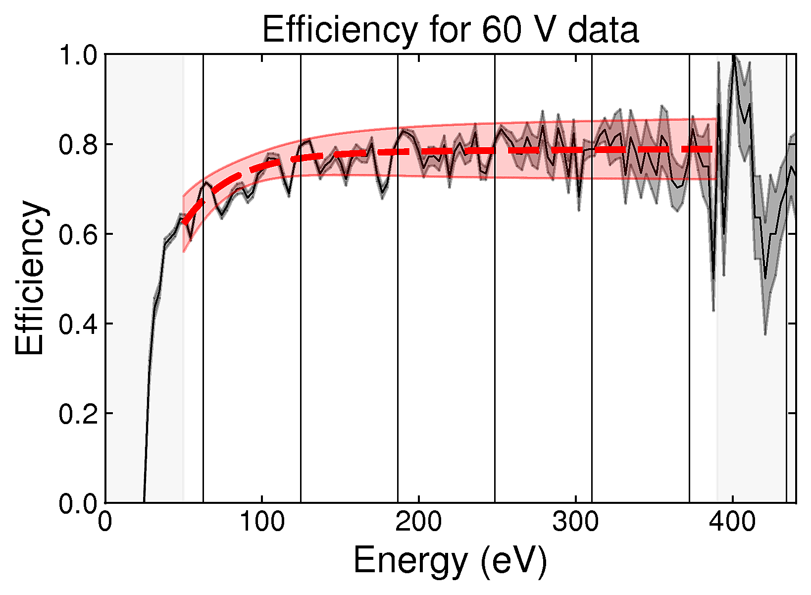
Trigger efficiency for the 100 V data
Top panel: comparison of the combined laser spectrum at 50 mK triggered with the laser TTL and triggered with the trigger used for the dark-matter-search data. Bottom panel: ratio of the histograms reported on the top panel, the trigger theshold at 50 mK is 29 eV. For this analysis, the lower limit of the region of interest was set at 50 eV to simplify the treatment of trigger effects. Note that the same procedure was applied to the 52 mK data and we found a threshold of 37 eV.

Efficiency
February 21st, 2020

Efficiency
February 21st, 2020

Data
March 27st, 2020
More HVeV Run 2
References for Fig. 30 and 31:
- SuperCDMS HVeV R1
- R. Agnese, et al. First dark matter constraints from a SuperCDMS single-charge sensitive detector. Phys. Rev. Lett., 121:051301, 2018.
- DAMIC
- A. Aguilar-Arevalo, et al. Constraints on light dark matter particles interacting with electrons from DAMIC at SNOLAB. Phys. Rev. Lett., 123:181802, 2019.
- SENSEI
- O. Abramoff, et al. SENSEI: Direct-detection constraints on sub-GeV dark matter from a shallow underground run using a prototype skipper CCD. Phys. Rev. Lett., 122:161801, 2019.
- XENON10
- R. Essig, et al. Newconstraints and prospects for sub-GeV dark matter scattering off electrons in XENON. Phys. Rev. D, 96:043017,2017.
- R. Essig, et al. First direct detection limits on sub-GeV dark matter from XENON10. Phys. Rev. Lett., 109:021301, 2012.
- XENON1T
- E. Aprile, et al. Light dark matter search with ionization signals in XENON1T. Phys. Rev. Lett., 123:251801,2019.
References for Fig. 32 and 33:
- SuperCDMS Soudan
- T. Aralis, et al. Constraints on dark photons and axion-like particles from SuperCDMS Soudan, arXiv: 1911.11905, 2019.
- XENON10 and XENON100
- I. M. Bloch, et al. Searching for dark absorption with direct detection experiments. J. High Energy Phys., 2017:1029, 2017.
- SuperCDMS HVeV R1
- R. Agnese, et al. First dark matter constraints from a SuperCDMS single-charge sensitive detector. Phys. Rev. Lett., 121:051301, 2018.
- DAMIC
- A. Aguilar-Arevalo, et al. Constraints on light dark matter particles interacting with electrons from DAMIC at SNOLAB. Phys. Rev. Lett., 123:181802, 2019.
- SENSEI
- O. Abramoff, et al. SENSEI: Direct-detection constraints on sub-GeV dark matter from a shallow underground run using a prototype skipper CCD. Phys. Rev. Lett., 122:161801, 2019.
- Stellar constraints
- H. An, et al. Direct detection constraints on dark photon dark matter. Phys. Lett. B, 747:331, 2015.
- N. Viaux, et al. Neutrino andaxion bounds from the globular cluster M5 (NGC 5904). Phys. Rev. Lett., 111:231301, 2013.
- M. Tanabashi, et al. Review of particle physics. Phys. Rev. D, 98:030001, 2018.
- M. M. Miller-Bertolami, et al. Revisiting the axion bounds from the galactic white dwarf luminosity function. JCAP, 1410:069, 2014.
References for Fig. 34:
- G. Hildebrandt et al. Normale und anomale Absorption von Röntgen-Strahlen in Germanium und Silicium/Normal and anomalous absorption of X-rays in Germanium and Silicon. Z. Naturforsch. A, 28:588, 1973.
- F. C. Brown and O. P. Rustgi. Extreme Ultraviolet Transmission of Crystalline and Amorphous Silicon. Phys. Rev. Lett., 28:497, 1972.
- C. Gahwiller and F. C. Brown. Photoabsorption near the LII, III Edge of Silicon and Aluminum. Phys. Rev. B, 2:1918, 1970.
- B. L. Henke et al. X-Ray Interactions: Photoabsorption, Scattering, Transmission, and Reflection at E =50-30,000 eV, Z = 1-92. At. Data Nucl. Data Tables, 54:181, 1993.
- W. Da-Chun et al. Measurement of the mass attenuation coefficients for SiH4 and Si. Nucl. Instrum. Meth. B., 95:161, 1995.
- M. A. Green and M. J. Keevers. Optical properties of intrinsic silicon at 300 K. Prog. Photovoltaics, 3:189, 1995.
- M. A. Green. Self-consistent optical parameters of intrinsic silicon at 300 K including temperature coefficients. Sol. Energy Mater. Sol. Cells, 92:1305, 2008.
- W. C. Dash and R. Newman. Intrinsic Optical Absorption in Single-Crystal Germanium and Silicon at 77 oK and 300 oK. Phys. Rev., 99:1151, 1955.
- D. F. Edwards.- Silicon (Si)*. In Edward D. Palik editor, Handbook of Optical Constants of Solids, pages 547 � 569. Academic Press, Burlington, 1997.
- G. G. Macfarlane et al. Fine Structure in the Absorption-Edge Spectrum of Si. Phys. Rev., 111:1245, 1958.
- S. E. Holland et al. Fully-depleted, back-illuminated charge-coupled devices fabricated on high-resistivity silicon. IEEE Trans. Electron Devices, 50:225, 2003.
- E. M. Gullikson et al. Absolute photoabsorption measurements of Mg, Al, and Si in the soft-x-ray region below the L2,3 edges. Phys. Rev. B, 49:16283, 1994.
- M. J. Berger et al. XCOM: Photon cross section database (version 1.5), 2010.
- F. C. Brown et al. L2,3 threshold spectra of doped siliconand silicon compounds. Phys. Rev. B, 15:4781, 1977.
- W. R. Hunter. Observation of Absorption Edges inthe Extreme Ultraviolet by Transmittance Measurements Through Thin Unbacked Metal Films.
- In F. Abelés, editor, Optical Properties and Electron Structure of Metals and Alloys, pages 136�146. North-Holland Publishing Company - Amsterdam, 1966.
- D. E. Aspnes and A. A. Studna. Dielectric functions andoptical parameters of Si, Ge, GaP, GaAs, GaSb, InP, InAs, and InSb from 1.5 to 6.0 eV. Phys. Rev. B, 27:985,1983.
- Y. Hochberg et al. Absorption of light dark matter insemiconductors. Phys. Rev. D, 95:023013, 2017.
- K. Rajkanan et al. Absorption coefficient of silicon for solar cell calculations. Solid State Electron., 22:793, 1979.